

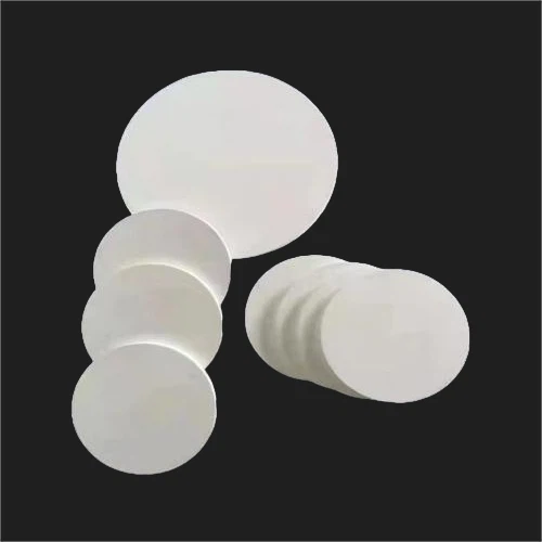
Meaning and Function of Boron Source
Boron source refers to the source of boron element for semiconductor materials. Boron, as an important doping element in semiconductor materials, can change the conductivity of semiconductor materials, improve its electron mobility, and thus optimize the performance of semiconductor devices. In the semiconductor manufacturing process, the quality and purity of the boron source directly affect the quality of semiconductor products.
Application of Boron Source in Semiconductor
In the semiconductor production process, the boron source usually exists in the form of compounds such as boric acid, borane, and boric ester. These boron compounds play a key role in different stages of the semiconductor production process, such as cleaning, doping, and ion implantation. For example, in the cleaning process, the boron source can remove organic pollutants and metal ions on the surface of the semiconductor; in the doping process, the boron source can change the conductivity type of the semiconductor; in the ion implantation process, the boron source can improve the stability of the ion beam.
Development of my country in the Field of Semiconductor Boron Source
Nowadays,China has achieved remarkable results in the research and production of Semiconductor Boron Source. In recent years, chinese semiconductor production are growing, and the demand for boron sources are increasing. In order to meet the domestic market demand, Chinese enterprises and scientific research institutions have increased their research on boron source materials and continuously improved the purity and performance of boron sources.
Semiconductor Boron Source Packaging and Transportation

Product packaging is in accordance with the "Technical Specifications" or industry standards;
The packaging of Semiconductor Boron Source meets the characteristics and performance of the product itself, including sufficient to prevent the product from moisture, rain, rust, corrosion, and shock, and can accept multiple handling, loading and unloading, and transportation;

Product Process and Production Flow
The production process of Semiconductor Boron Source includes key steps such as raw material selection, boron nitride powder preparation, molding, sintering treatment, and post-processing and testing. Each step requires strict control of process parameters and operating conditions to ensure the quality and performance of the final product. With the advancement of science and technology and the continuous optimization of processes, the production process of boron nitride ceramics will continue to be improved and perfected to provide better material support for the development of various industries.
Performance Parameters
|
chemical components BN% |
% |
99 |
|
Other Ingredients |
no |
|
|
density |
g/cm3 |
>2 |
|
Leeb hardness |
HL |
300 |
|
Bending strength |
Mpa |
35 |
|
Thermal expansion coefficient (25℃-1200℃) |
(10-6/K) |
-1~2.5 |
|
Thermal conductivity (room temperature) |
W/mk |
50 |
|
Operating temperature |
℃ |
Above 2000℃ (vacuum or gas protection) |
|
Room temperature resistivity |
Ω. cm |
>1014 |
Hot Tags: semiconductor boron source, China semiconductor boron source manufacturers, suppliers, factory, Semiconductor Boron Source, Boron Nitride Composite Ceramics, Titanium Diboride Powder, Boron Carbide Granules, Ceramic Evaporation Boat, training boron nitride


